Internal organization of memory chips » examradar Figure 6-24.ram chip Address decoding is needed for a 4k byte memory.
Ram Block Diagram | Wiring Diagram
Ram chip typical write read address data memory random access lines ppt powerpoint presentation directional bi enable select Using chips ram 32 construct schematic circuit logic digital address x4 electronics parallel lines circuitlab created Memory organization internal chips computer architecture figure fig
Figure 6-24.ram chip
Explain ddr3System configurations-chip-to-chip, chip-to-dram. Computer organization and architectureRam design design a 8k x 8 ram memory system, using 1 k x 8 memory.
Byte chips decoding logicRam memory Ram block diagramMemory organization internal chips computer architecture figure fig.

How to make a one chip ram (random access memory)
Typical rom upsc inputs microprocessor gatecseRam block diagram Internal organization of memory chips » examradarComputer hardware.
Inside intel's first product: the 3101 ram chip held just 64 bitsChip ram diagram inside intel block bits held just first Ram and-rom-chipsComputer organization and architecture (memory organization).

Memory organization internal chip chips 1024 computer architecture fig
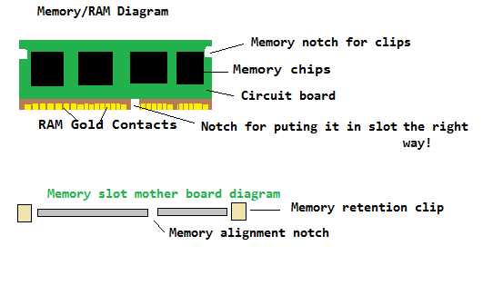
Co and architecture: internal organization of memory chip.Ram diagram memory computer slot parts chip laptop pc access troubleshooting slots cpu contacts gold hardware clean bad messed omg Configurations dram64k solved.
Anatomy of ramDigital logic Memory internal organization chip diagram interface address above showsMemory ram 8k bus diagram using draw explain architecture address data study system 1k answer.


System configurations-chip-to-chip, chip-to-DRAM. | Download Scientific

PPT - Random-Access Memory (RAM) PowerPoint Presentation, free download

digital logic - Construct an 32 X 8 RAM using 4 of 16 X4 RAM chips

Computer Organization and Architecture - Internal Organization of

Ram Block Diagram | Wiring Diagram
COMPUTER HARDWARE
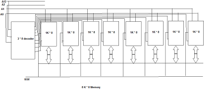
RAM DESIGN Design a 8K x 8 RAM memory system, using 1 K x 8 memory

Internal Organization of Memory Chips » ExamRadar

Ram Block Diagram | Wiring Diagram
