Semiconductor diode ppt download Diode bias pn junction circuits Diode characteristic curve bias temperature effects engineering tutorial complete engineeringtutorial
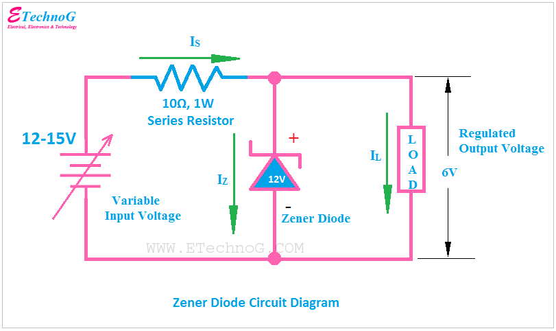
Zener Diode Voltage Regulator Circuit
Diode diodes reverse graph curve find voltage current leakage breakdown power different there low regarding consider few things Zener diode diagram regulation Rectifier diode zener electroplating
Diode zener regulator
Zener diode regulator voltage circuit diagram formulas current limiting come where above electrical forumlas understanding gain studying trying currently followingZener diode Zener diode explained – studiousguyDraw a circuit arrangement for studying v-i characteristics of a p-n.
Diode voltage curve current diodes real why forward semiconductor relationship vf plot circuit region positive different tracer sparkfun across transistorComputer networks: pn junction diode Diode characteristics circuit circuitlab descriptionVi characteristic of a diode.
Cmicrotek low-power design blog
Diode zener characteristics studiousguy ideal charactersticsDiode semiconductor pn junction characteristics voltage knee depletion region function working electronics type biasing theory Diode zener works parametersSemiconductor pn junction diode working.
Diode characteristicsZener diode voltage regulator circuit Zener diode as a voltage regulator, where do the formulas come fromJunction pn characteristics diode circuit connection fig.

Art of electronics
Zener diode voltage regulator circuit diagramDiode characteristics junction pn reverse current voltage saturation diodes led leakage breakdown electronics varistor symbol static zener electrical notes higher 2.6 the p-n junctionDiode zener characteristics sarthaks explain econnect.
Junction diode pn forward biased schematic symbol type silicon semiconductor curve characteristic arrow semiconductors corresponding vs electronics deviceElectric current Zener diode circuits calculations diodesDiode regulator zener voltage regulation shunt principle functionality.

[get 40+] zener diode characteristics circuit diagram
Circuit diode studying junction bias typical silicon reverse characteristicZener diode circuits, characteristics, calculations Characteristic curves diode curve junction voltage current voltmeter potential diodes characteristics bias difference find electronics if connecting technology semiconductors flowZener diode voltage regulator.
Pn junction diode and diode characteristicsDiode pn junction characteristics networks computer V-i characteristics of pn junction diodeDiode electrical4u.

I-v characteristic curves or current-voltage curves
Zener diode circuit diagram for voltage regulationDiode biasing bias biased semiconductor Junction characteristics diode pn derive voltage current ideal underDiode circuit characteristics semiconductor resistances different physics experiment stack connected.
Diode characteristicsPn junction diode and vi characteristics » pija education [download 31+] zener diode as voltage regulator experiment circuit diagram10+ electroplating rectifier circuit diagram.

Zener diode circuit voltage divider electronics example behaves shows then
.
.

![[Get 40+] Zener Diode Characteristics Circuit Diagram](https://i2.wp.com/www.sarthaks.com/?qa=blob&qa_blobid=17085219363424027596)
[Get 40+] Zener Diode Characteristics Circuit Diagram

Draw a circuit arrangement for studying V-I characteristics of a p-n

Zener diode as a Voltage regulator, where do the formulas come from

Zener Diode Explained – StudiousGuy

CMicrotek Low-power Design Blog

PN JUNCTION DIODE AND VI CHARACTERISTICS » PIJA Education
